
Researchers from the University of Warwick have developed a way to deform the p-type and n-type semiconductors in solar cells to improve their efficiency and generate more electrical energy from sunlight.

Published in Science, the report ‘Flexo-Photovoltaic Effect’ describes the structure of most commercial solar cells, which places an absolute limit on their effectiveness.
“There are engineering challenges but it should be possible to create solar cells where a field of simple glass based tips could be held in tension to sufficiently de-form each semiconductor crystal,” said department of physics professor Marin Alexe.
“If such future engineering could add even a single percentage point of efficiency it would be of immense commercial value to solar cell manufacturers and power suppliers.”
Most solar cells are formed of two layers, creating a junction at the boundary where positively-charged p-type and negatively-charged n-type semiconductors meet. Negatively-charged electrons are carried by n-type semiconductors towards p-type semiconductors which have holes for them to fill.
How well do you really know your competitors?
Access the most comprehensive Company Profiles on the market, powered by GlobalData. Save hours of research. Gain competitive edge.

Thank you!
Your download email will arrive shortly
Not ready to buy yet? Download a free sample
We are confident about the unique quality of our Company Profiles. However, we want you to make the most beneficial decision for your business, so we offer a free sample that you can download by submitting the below form
By GlobalDataWhen the cell absorbs light, the junction splits the photo-excited carriers in opposite directions, generating current and voltage. This junction is integral to producing electricity, but contains an inherent limit – the Shockley-Queisser Limit – which means that even in ideal conditions only a maximum of 33.7% of power contained in sunlight can ever be converted into electricity.
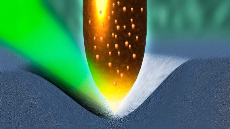
Some materials have been known to collect charges another way, known as the bulk photovoltaic effect, due to their lack of perfect symmetry around their central point, which allows the generation of voltage higher than would otherwise be expected. While many of these materials are themselves inefficient in regards to power generation, the Warwick team experimented with altering the shape of high-efficiency semiconductors to maximise their potential for generating electricity.
The researchers used conductive tips to force semiconductors into a device called a nano-indenter, which they used to deform individual crystals of silicon, strontium titanate and titanium dioxide. They found that all three could be deformed to provide the bulk photovoltaic effect, which occurs in non-symmetrical semiconductors.
“Extending the range of materials that can benefit from the bulk photovoltaic effect has several advantages,” said Alexe.
“It is not necessary to form any kind of junction; any semiconductor with better light absorption can be selected for solar cells, and finally, the ultimate thermodynamic limit of the power conversion efficiency, so-called Shockley-Queisser Limit, can be overcome.”