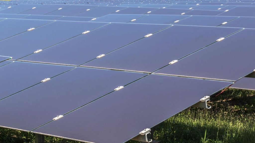
JA Solar Technology has filed a patent for a silicon wafer with an innovative design to increase the efficiency of photovoltaic modules. The wafer includes an extension edge for reduced sheet gaps and increased power generation area. The patent claims are not disclosed. GlobalData’s report on JA Solar Technology gives a 360-degree view of the company including its patenting strategy. Buy the report here.
According to GlobalData’s company profile on JA Solar Technology, Smart factory applications was a key innovation area identified from patents. JA Solar Technology's grant share as of January 2024 was 66%. Grant share is based on the ratio of number of grants to total number of patents.
Monocrystalline silicon wafer with extension edge for photovoltaic modules
See Also:
A recently filed patent (Publication Number: US20230378387A1) describes a unique monocrystalline silicon wafer designed for efficient welding during manufacturing processes. The wafer includes a silicon wafer main body with an extension edge that extends outward from the main body, forming a ribbon-shaped structure parallel to the main body's edge. This extension edge is specifically designed to overlap below an adjacent monocrystalline silicon wafer during the welding process. The main body and extension edge are cut and shaped from a squared monocrystalline silicon rod, with specific dimensions and geometries outlined in the patent claims.
Furthermore, the patent also details a method for preparing these monocrystalline silicon wafers, involving axial cutting and radial line cutting on the silicon rod to obtain the desired wafer shapes. Additionally, the patent discusses the use of these wafers in the formation of a cell string through stitch-welding several cell slices. These cell slices are obtained by cutting a cell sheet made of the monocrystalline silicon wafer, with specific texturing, diffusing, etching, and coating steps involved in the process. The resulting cell string includes extension edges that overlap below adjacent cell slices, with specific dimensions and configurations outlined in the patent claims for optimal performance and efficiency in power generation applications.
To know more about GlobalData’s detailed insights on JA Solar Technology, buy the report here.
Premium Insights
From

The gold standard of business intelligence.
Blending expert knowledge with cutting-edge technology, GlobalData’s unrivalled proprietary data will enable you to decode what’s happening in your market. You can make better informed decisions and gain a future-proof advantage over your competitors.


